Pinout
This pinout works for all boards. You can also copy values from custom_board.h (see jorne_ble.c macros implementation).
| nRFMicro | nice!nano | ProMicro | Left | Right | ProMicro | nice!nano | nRFMicro |
|---|---|---|---|---|---|---|---|
| P0.06 | P0.06 | D3 | PIN1 | PIN24 | RAW | RAW | RAW |
| P0.08 | P0.08 | D2 | PIN2 | PIN23 | GND | GND | GND |
| GND | GND | GND | PIN3 | PIN22 | RST | P0.18 | P0.18 |
| GND | GND | GND | PIN4 | PIN21 | VCC | VCC | VCC |
| P0.15 | P0.17 | D1 | PIN5 | PIN20 | F4 | P0.31 | P0.30 |
| P0.17 | P0.20 | D0 | PIN6 | PIN19 | F5 | P0.29 | P0.31 |
| P0.20 | P0.22 | D4 | PIN7 | PIN18 | F6 | P0.02 | P0.29 |
| P0.13 | P0.24 | C6 | PIN8 | PIN17 | F7 | P1.15 | P0.02 |
| P0.24 | P1.00 | D7 | PIN9 | PIN16 | B1 | P1.13 | P1.13 |
| P0.09 | P0.11 | E6 | PIN10 | PIN15 | B3 | P1.11 | P0.03 |
| P0.10 | P1.04 | B4 | PIN11 | PIN14 | B2 | P0.10 | P0.28 |
| P1.06 | P1.06 | B5 | PIN12 | PIN13 | B6 | P0.09 | P1.11 |
- P0.18 - RESET
- P1.10 - BLUE_LED (P0.15 on nice!nano)
- P1.09 - POWER_PIN (EXT_VCC control since 1.0, P0.13 on nice!nano) (1-off, 0-on)
- P0.26 - SWITCH_PIN (battery on/off state, from 0.03 to 1.1)
- P0.04 - BATTERY_PIN (analog battery voltage in mV, since 1.1, MUST BE analog pin, e.g. P0.04 is AIN2)
- P0.05 - PROG_PIN (charger prog pin, 1.2-1.3 only, set to 0 or internal 13K pull-down for charging)
- P0.07 - STAT_PIN (charger stat pin, 1.2 only, mostly unused)
These pins are available on the back side via through hole pads:
- P1.04
- P1.02
- P1.00
- P0.22
- P0.12
- P0.26 (free since 1.2)
- P0.07 (free since 1.3)
These pins are free on the top side of the module:
- P0.00 (XL1)
- P0.01 (XL2)
- P0.05 (free since 1.4)
So there are 10 free pins (including top side). Revision 1.4 may use P0.00 and P0.01 with the Crystal (you can desolder it).

These pins can be used to enter OTA mode (see Bootloader):
- P1.02 DFU (BUTTON_1)
- P0.12 FRST (BUTTON_2)
The underside unused pin P0.12 (apparently) cannot be used for I2C which has pull-down resistors. This pin is used by (PCA10056) bootloader. Doing so results in continuous looping of dfu bootloader mode. You might need to choose the appropriate bootloader that doesn't use this pin as FRST button (or maybe just don't use pull-down resistors). See Bootloader.
You're not supposed to use low drive pins for I2C protocol and RGB data (though I think I2C OLEDs are fine, they're sub-10kHz).
They are actually "standard drive, low frequency" pins. They can be found in the nRF52840 Product Specification (page 576):
Normal (high frequency) pins are:
- P0.00, P0.01, P0.26, P0.27, P0.04, P0.05, P0.06, P0.07, P0.08, P1.08, P1.09, P0.11, P0.12, P0.14, P0.16, P0.18, P0.19, P0.21, P0.23, P0.25, P0.13, P0.15, P0.17, P0.20, P0.22, P0.24, P1.00
Low drive (low frequency) pins are:
- P0.31, P0.29, P0.02, P1.15, P1.13, P1.10, P0.30, P0.28, P0.03, P1.14, P1.12, P1.11, P0.10, P0.09, P1.07, P1.06, P1.05, P1.04, P1.03, P1.02, P1.01
Pins AIN0-AIN7 may be used as analog input.
nRF52840 pin assignments (click to expand)
| Pin | Name | Function | Description | Recommended usage |
|---|---|---|---|---|
| A8 | P0.31 (AIN7) | Digital I/O | General purpose I/O | Standard drive, low frequency I/O only |
| A10 | P0.29 (AIN5) | Digital I/O | General purpose I/O | Standard drive, low frequency I/O only |
| A12 | P0.02 (AIN0) | Digital I/O | General purpose I/O | Standard drive, low frequency I/O only |
| A14 | P1.15 | Digital I/O | General purpose I/O | Standard drive, low frequency I/O only |
| A16 | P1.13 | Digital I/O | General purpose I/O | Standard drive, low frequency I/O only |
| A18 | Dec 02 | Power | 1.3 V regulator supply decoupling | |
| A20 | P1.10 | Digital I/O | General purpose I/O | Standard drive, low frequency I/O only |
| A22 | VDD | Power | Power supply | |
| A23 | XC2 | Analog input | Connection for 32 MHz crystal | |
| B1 | VDD | Power | Power supply | |
| B3 | DCC | Power | DC/DC converter output | |
| B5 | Dec 04 | Power | 1.3 V regulator supply decoupling | |
| B7 | VSS | Power | Ground | |
| B9 | P0.30 (AIN6) | Digital I/O | General purpose I/O | Standard drive, low frequency I/O only |
| B11 | P0.28 (AIN4) | Digital I/O | General purpose I/O | Standard drive, low frequency I/O only |
| B13 | P0.03 (AIN1) | Digital I/O | General purpose I/O | Standard drive, low frequency I/O only |
| B15 | P1.14 | Digital I/O | General purpose I/O | Standard drive, low frequency I/O only |
| B17 | P1.12 | Digital I/O | General purpose I/O | Standard drive, low frequency I/O only |
| B19 | P1.11 | Digital I/O | General purpose I/O | Standard drive, low frequency I/O only |
| B24 | XC1 | Analog input | Connection for 32 MHz crystal | |
| C1 | Dec 01 | Power | 1.1 V regulator supply decoupling | |
| D2 | P0.00 (XL1) | Digital I/O | General purpose I/O | |
| D23 | Dec 03 | Power | Power supply, decoupling | |
| E24 | Dec 06 | Power | 1.3 V regulator supply decoupling | |
| F2 | P0.01 (XL2) | Digital I/O | General purpose I/O | |
| F23 | VSS_PA | Power | Ground (radio supply) | |
| G1 | P0.26 | Digital I/O | General purpose I/O | |
| H2 | P0.27 | Digital I/O | General purpose I/O | |
| H23 | ANT | RF | Antenna connection | See Reference circuitry on page 583 |
| J1 | P0.04 (AIN2) | Digital I/O | General purpose I/O | |
| J24 | P0.10 (NFC2) | Digital I/O | General purpose I/O | Standard drive, low frequency I/O only |
| K2 | P0.05 (AIN3) | Digital I/O | General purpose I/O | |
| L1 | P0.06 | Digital I/O | General purpose I/O | |
| L24 | P0.09 (NFC1) | Digital I/O | General purpose I/O | Standard drive, low frequency I/O only |
| M2 | P0.07 | Digital I/O | General purpose I/O | |
| N1 | P0.08 | Digital I/O | General purpose I/O | |
| N24 | Dec 05 | Power | 1.3 V regulator supply decoupling | |
| P2 | P1.08 | Digital I/O | General purpose I/O | |
| P23 | P1.07 | Digital I/O | General purpose I/O | Standard drive, low frequency I/O only |
| R1 | P1.09 | Digital I/O | General purpose I/O | |
| R24 | P1.06 | Digital I/O | General purpose I/O | Standard drive, low frequency I/O only |
| T2 | P0.11 | Digital I/O | General purpose I/O | |
| T23 | P1.05 | Digital I/O | General purpose I/O | Standard drive, low frequency I/O only |
| U1 | P0.12 | Digital I/O | General purpose I/O | |
| U24 | P1.04 | Digital I/O | General purpose I/O | Standard drive, low frequency I/O only |
| V23 | P1.03 | Digital I/O | General purpose I/O | Standard drive, low frequency I/O only |
| W1 | VDD | Power | Power supply | |
| W24 | P1.02 | Digital I/O | General purpose I/O | Standard drive, low frequency I/O only |
| Y2 | VDDH | Power | High voltage power supply | |
| Y23 | P1.01 | Digital I/O | General purpose I/O | Standard drive, low frequency I/O only |
| AA24 | SWDCLK | Debug | Serial wire debug clock input | |
| AB2 | DCCH | Power | DC/DC converter output | |
| AC5 | DECUSB | Power | 3.3 V regulator supply decoupling | |
| AC9 | P0.14 | Digital I/O | General purpose I/O | |
| AC11 | P0.16 | Digital I/O | General purpose I/O | |
| AC13 | P0.18 nRESET | Digital I/O | General purpose I/O | QSPI/CSN |
| AC15 | P0.19 | Digital I/O | General purpose I/O | QSPI/SCK |
| AC17 | P0.21 | Digital I/O | General purpose I/O | QSPI |
| AC19 | P0.23 | Digital I/O | General purpose I/O | QSPI |
| AC21 | P0.25 | Digital I/O | General purpose I/O | |
| AC24 | SWDIO | Debug | Serial wire debug I/O | |
| AD2 | VBUS | Power | 5 V input for USB 3.3 V regulator | |
| AD4 | D- | Digital I/O | USB D- | USB |
| AD6 | D+ | Digital I/O | USB D+ | USB |
| AD8 | P0.13 | Digital I/O | General purpose I/O | |
| AD10 | P0.15 | Digital I/O | General purpose I/O | |
| AD12 | P0.17 | Digital I/O | General purpose I/O | |
| AD14 | VDD | Power | Power supply | |
| AD16 | P0.20 | Digital I/O | General purpose I/O | |
| AD18 | P0.22 (AD20) | Digital I/O | General purpose I/O | QSPI |
| AD22 | P1.00 | Digital I/O | General purpose I/O | QSPI |
| AD23 | VDD | Power | Power supply |


See Components#alternative-modules for prices and links to IPEX antennas and stuff.
E73-2G4M08S1CX schematic (with the IPEX antenna) is IDENTICAL. Does not need an extra XTAL or anything.
nRF52833-based (half the Flash, so no Python). Lacks pin 1.11 so it's not 100% compatible. Also no DCCH so DC-DC mode.
Other changes for nRF52833 module is that 1.10 is now 0.25 (blue led) and 1.13 is now 1.05 (standard gpio).

Since pad 1 - P1.11 is NC - Not Connected on E73-2G4M08S1E, you can add a connection from P1.04 to P1.11:

So it would still need PCB mod (or a wire jumper) and a firmware patch (there's also too little Flash). ZMK support was added just recently.
nRF52840 supports Normal and High Voltage power supply modes. The latter is either internal LDO or internal DC-DC.
- Normal mode uses VDD pin (shorted with VDDH pin). It's usually powered via an external LDO (1.8-3.6V).
- HV Mode with internal LDO uses VDDH only (1.8-5.5V), sets 1.8V core voltage (3.3V with UICR_REGOUT0_VOUT_3V3).
- HV Mode with internal DC-DC uses VDDH pin and 10uH on DCCH and VDD (enable with BOARD_ENABLE_DCDC_HV).
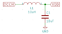
If you don't want to add 10uH inductor you can use internal LDO and leave DCCH and VDD pins hanging. Using the internal DCDC is better when you have high current draws, such as the radio TX current spikes. We don't need that if we power high current components (OLED/RGB) separately (via a separate power bus). Note that internal regulators only support up to 25 mA.
- USB won't power up the board from a single VUSB pin, you also have to supply power to the core using methods above.
- Some Nordic products (e.g. nRF52833) have no DC-DC and no DCCH pin so you're limited to internal LDO and VDD.
- Some modules (e.g. Holyot YJ-18010) don't route out existing DCCH and VDDH pins, so you're limited to VDD.
nRFMicro 1.4 historically uses VDD (external LDO), but it's a subject to change for the future versions.
Besides QFN-73 there is QFN-40 version of nRF52833 you can use it for handsoldering.
There are 18 routed out GPIO pins: P0.00, P0.01, P0.04, P0.05, P1.09, P0.11, P0.15, P0.17, P0.18, P0.20, P0.09, P0.10, P0.03, P0.02, P0.28, P0.29, P0.30, P0.31.
Note that P0.18/RESET, P0.00/XL1, P0.01/XL2 are usually reserved for RESET and optional crystal (XTAL).
It also has 22 service pins: DEC1, VDD, VDDH, VBUS, DECUSB, D-, D+, VDD, SWDIO, SWDCLK, DEC5, ANT, VSS_PA, DEC6, DEC3, XC1, XC2, VDD, VSS, DEC4, DCC, VDD.

nRF52833 QFN40 pin assignments (click to expand)
| Pin | Name | Function | Description | Recommended usage |
|---|---|---|---|---|
| 1 | DEC1 | Power | 1.1 V Digital supply decoupling | |
| 2 | P0.00 XL1 |
Digital I/O Analog input |
General purpose I/O pin. Connection for 32.768 kHz crystal |
|
| 3 | P0.01 XL2 |
Digital I/O Analog input |
General purpose I/O pin Connection for 32.768 kHz crystal |
|
| 4 | P0.04 AIN2 |
Digital I/O Analog input |
General purpose I/O pin Analog input |
|
| 5 | P0.05 AIN3 |
Digital I/O Analog input |
General purpose I/O pin Analog input |
|
| 6 | P1.09 | Digital I/O | General purpose I/O pin | |
| 7 | P0.11 | Digital I/O | General purpose I/O pin | |
| 8 | VDD | Power | Power supply | |
| 9 | VDDH | Power | High voltage power supply | |
| 10 | VBUS | Power | 5 V input for USB 3.3 V regulator | |
| 11 | DECUSB | Power | USB 3.3 V regulator supply decoupling | |
| 12 | D- | USB | USB D- | |
| 13 | D+ | USB | USB D+ | |
| 14 | P0.15 | Digital I/O | General purpose I/O | |
| 15 | P0.17 | Digital I/O | General purpose I/O | |
| 16 | P0.18 nRESET |
Digital I/O | General purpose I/O Configurable as pin RESET |
|
| 17 | P0.20 | Digital I/O | General purpose I/O | |
| 18 | VDD | Power | Power supply | |
| 19 | SWDIO | Debug | Serial wire debug I/O for debug and programming | |
| 20 | SWDCLK | Debug | Serial wire debug clock input for debug and programming | |
| 21 | DEC5 Not connected |
Power | 1.3 V regulator supply decoupling for build codes Axx and earlier. Not connected for build codes Bxx and later. |
|
| 22 | P0.09 NFC1 |
Digital I/O NFC input |
General purpose I/O NFC antenna connection |
Standard drive, low frequency I/O only |
| 23 | P0.10 NFC2 |
Digital I/O NFC input |
General purpose I/O NFC antenna connection |
Standard drive, low frequency I/O only |
| 24 | ANT | RF | Single-ended radio antenna connection | See Reference circuitry for guidelines on how to ensure good RF performance |
| 25 | VSS_PA | Power | Ground (radio supply) | |
| 26 | DEC6 | Power | 1.3 V regulator supply decoupling | Must be connected to DEC4 (pin 38) |
| 27 | DEC3 | Power | Power supply, decoupling | |
| 28 | XC1 | Analog input | Connection for 32 MHz crystal | |
| 29 | XC2 | Analog input | Connection for 32 MHz crystal | |
| 30 | VDD | Power | Power supply | |
| 31 | P0.03 AIN1 |
Digital I/O Analog input |
General purpose I/O pin Analog input |
Standard drive, low frequency I/O only |
| 32 | P0.02 AIN0 |
Digital I/O Analog input |
General purpose I/O pin Analog input |
Standard drive, low frequency I/O only |
| 33 | P0.28 AIN4 |
Digital I/O Analog input |
General purpose I/O pin Analog input |
Standard drive, low frequency I/O only |
| 34 | P0.29 AIN5 |
Digital I/O Analog input |
General purpose I/O pin Analog input |
Standard drive, low frequency I/O only |
| 35 | P0.30 AIN6 |
Digital I/O Analog input |
General purpose I/O pin Analog input |
Standard drive, low frequency I/O only |
| 36 | P0.31 AIN7 |
Digital I/O Analog input |
General purpose I/O pin Analog input |
|
| 37 | VSS | Power | Ground | |
| 38 | DEC4 | Power | 1.3 V regulator supply decoupling | Must be connected to DEC6 (pin 26) |
| 39 | DCC | Power | DC/DC converter output | |
| 40 | VDD | Power | Power supply | |
| Die pad | VSS | Power | Ground pad | Exposed die pad must be connected to ground (VSS) for proper device operation |
- https://infocenter.nordicsemi.com/pdf/nRF52840_PS_v1.1.pdf (nRF52840 Product Specification)